When standard trays can't handle deep-draw, high-density vertical insertion — engineered thermoforming can.
The Packaging Challenge in PCBA Logistics
As electronic assemblies grow denser and more sensitive, the packaging that protects them during storage and transit must keep pace. For PCBA (Printed Circuit Board Assembly) boards, two requirements frequently collide:
1. 1.Maximize quantity per tray — reducing packaging cost per unit and improving logistics efficiency.
2. 2.Vertical (edge-standing) insertion — required when component height profiles or soldering joints make flat stacking risky.
Vertical insertion dramatically increases tray depth relative to footprint, which introduces a well-known thermoforming obstacle: deep-draw demolding. The deeper the cavity, the harder it is to maintain uniform wall thickness and release the part cleanly from the mold. Many suppliers avoid this geometry altogether, or compromise on capacity.
Material Selection: Why ESD HIPS?
High Impact Polystyrene (HIPS) with a permanent ESD (Electrostatic Dissipative) additive is the workhorse material for electronics packaging trays. Here's why it stands out:
|
Property |
Specification |
Why It Matters |
|
Surface Resistance |
10⁵–10⁹ Ω |
Falls squarely within the ESD-dissipative range per ANSI/ESD S541, safely bleeding off charge without sudden discharge |
|
Material Color |
Carbon-black filled (Black) |
Provides consistent, permanent ESD performance — not a topical coating that wears off |
|
Sheet Gauge |
2.2 mm (pre-form) → ~1.5 mm (finished wall) |
Thick enough for structural rigidity under stacking loads while remaining thermoformable in deep-draw geometries |
|
Thermoformability |
Excellent |
HIPS offers a wide forming window, critical for achieving uniform wall distribution in deep cavities |
Compared to alternatives:
· •PET/PETG: Higher clarity but narrower forming window; difficult in deep-draw.
· •PP: Good chemical resistance but poorer dimensional stability; ESD grades are costlier.
· •PS (General Purpose): Too brittle for stacking and repeated handling.
ESD HIPS strikes the optimal balance of formability, mechanical strength, ESD performance, and cost.
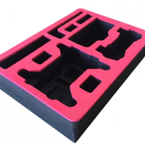
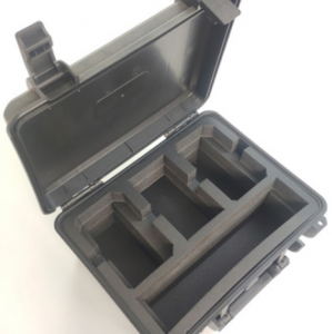
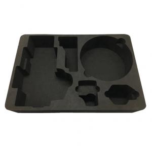
Engineering Deep-Draw Vertical-Insertion Trays
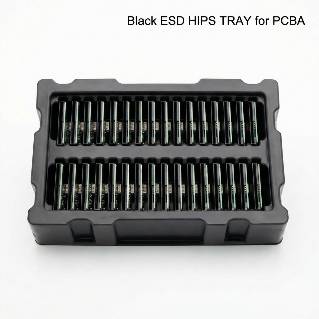
The core technical challenge: fitting 32 vertical PCBA slots into a compact 280 × 180 × 58 mm tray envelope — with reliable demolding.
Key Design Considerations
1. Draw Ratio Management
A 58 mm cavity depth against a 280 × 180 mm footprint yields a moderate overall draw ratio. However, individual slot cavities (narrow, deep channels for edge-standing PCBAs) push local draw ratios much higher. Our approach:
· •Optimized draft angles on each slot wall (typically 3°–5°) to facilitate mold release without wasting plan-view space.
· •Radiused transitions at cavity bottoms to prevent thinning and stress concentration.
2. Wall Thickness Control
Starting from a 2.2 mm sheet, the forming process stretches material into cavities. Maintaining ≥1.5 mm finished wall thickness across 32 deep slots requires:
· •Precise plug-assist pre-stretching to distribute material before final vacuum draw.
· •Controlled heating profiles to ensure uniform sheet temperature across the forming zone.
3. Stacking Architecture
The trays are designed for 180° nesting — rotating every other tray to interlock. Three loaded trays stack to approximately 160 mm total height, enabling efficient use of standard ESD bins and shipping containers.
4. Slot Geometry for PCBA Protection
Each of the 32 positions features:
· •Controlled-width channels matching the PCB edge thickness.
· •Support ribs preventing board-to-board contact.
· •Sufficient clearance for protruding components on the populated side.
Performance Summary
|
Parameter |
Value |
|
Material |
Black ESD HIPS (permanent carbon-loaded) |
|
Finished Wall Thickness |
1.5 mm |
|
Outer Dimensions |
280 × 180 × 58 mm |
|
Surface Resistance |
10⁵–10⁹ Ω |
|
Capacity |
32 PCS per tray |
|
Stacking |
180° rotation nesting; 3 trays ≈ 160 mm height |
When to Specify ESD HIPS Deep-Draw Trays
This tray design is particularly suited for:
· •SMT production lines handling populated PCBAs between process steps.
· •Incoming/outgoing inspection where boards must be individually accessible.
· •Warehousing and shipping of ESD-sensitive assemblies in controlled environments.
· •Any scenario where flat-lay trays waste space due to tall component profiles.
Conclusion
Deep-draw thermoforming of ESD HIPS is not a commodity process — it requires precise tooling design, material expertise, and process control to deliver trays that are compact yet high-capacity, structurally sound yet easily demolded. If your PCBA packaging demands vertical insertion and maximum density in a small footprint, this is the proven approach.
Contact us for a custom tray design consultation — from DFM review to sampling in days, not weeks.
�� Contact Us
YUFA Polymer Products Co., Ltd.�� Address: Shenzhen, China
�� Email: info@yufapolymer.com
�� Web: www.yufapolymer.com