Original blog by YUFA Polymer Products Co., Ltd.
�� Production Site: Shenzhen, China
�� info@yufapolymer.com | �� www.yufapolymer.com.
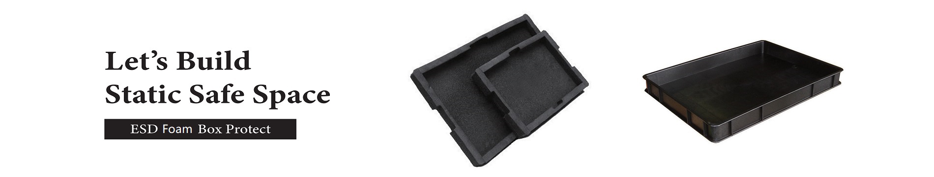
⏳ 1. Why Conductive EVA Foam Is Needed in High-End Industries
As semiconductor chips and optical modules become smaller, faster, and more sensitive, the risks associated with electrostatic discharge (ESD) grow exponentially. In these industries, even a microsecond of uncontrolled static charge can permanently destroy an IC or impair a laser diode.
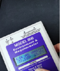
Conductive EVA foam (surface resistance: 10³–10⁶ Ω) provides a permanent, low-resistance path to ground. Compared with anti static EVA foam (10⁵–10⁹ Ω), it offers a faster and more reliable discharge, which is critical for semiconductor packaging and optoelectronic device protection..
�� 2. Typical Applications of Conductive EVA Foam
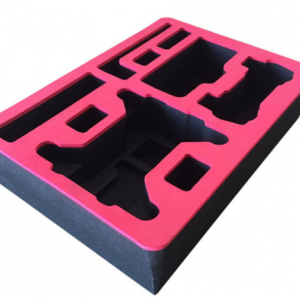
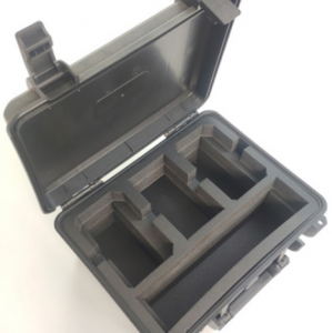
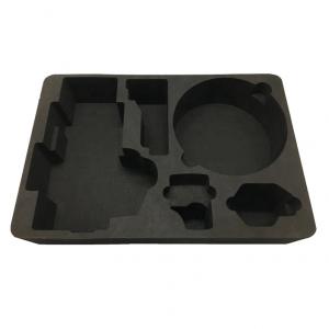
Conductive EVA foam is widely adopted in industries where static safety must be absolute:
· Semiconductor packaging – For wafers, ICs, TDMA network cards, and AI chips.
· Optoelectronic modules – Safeguarding optical transceivers, LD/PD chips, and laser assemblies.
· Precision PCBA handling – Protecting exposed circuit boards in testing and transport.
· Robotics & AI equipment – Conductive EVA trays for camera modules and robotic sensors.
· Cleanroom logistics – As conductive cushioning material in returnable containers.
In all these cases, conductive EVA foam ensures both cushioning and controlled ESD protection, making it indispensable for advanced manufacturing.
⚙️ 3. Customer Pain Points Solved
Electronics manufacturers and semiconductor suppliers choose conductive EVA foam to address:
· Elimination of static buildup – Immediate charge dissipation prevents latent failures.
· Safe handling of exposed pins and contacts – Prevents arcing during transport.
· Consistent resistance values – Reliable performance in both humid and dry environments.
· Compatibility with cleanroom standards – Dust-free and non-contaminating packaging solution.
By comparison, anti static EVA foam may be better for general electronics packaging, but conductive EVA foam is essential when zero tolerance for static damage is required.
�� 4. Technical Highlights
· Hardness: 38 Shore C (standard, customizable available)
· Color: Black
· Density: Custom per requirement
· Surface resistance: 10³–10⁶ Ω (permanent conductivity)
· Processing: CNC cutting, die-cutting, lamination, adhesive backing, insert fabrication
�� 5. Industry Value & Market Trend
The global demand for conductive EVA foam is increasing due to the growth of:
· AI semiconductor chips – requiring ultra-reliable ESD packaging foam solutions.
· 5G and high-speed optics – where optical modules must be transported in conductive carriers.
· Medical and laboratory instruments – ensuring safe packaging for diagnostic sensors.
As automation and robotics expand, conductive EVA foam will remain the premium choice for ESD packaging foam in high-value industries.
�� 6. Final Thought
When it comes to protecting semiconductors and optical devices, anti static EVA foam may not be enough. Only conductive EVA foam provides the low-resistance, permanent ESD protection required for the most sensitive applications.
At YUFA Polymer, we customize conductive EVA foam solutions to fit semiconductor trays, optoelectronic carriers, and robotics packaging systems.
�� Contact us today to discuss your ESD protection needs:
�� info@yufapolymer.com
�� www.yufapolymer.com