Why 450°C halogen-free silicone mats are replacing conventional workstation mats in high-reliability electronics manufacturing
1. The Hidden Challenge of Lead-Free Soldering
Lead-free soldering has become the global standard in electronics manufacturing, driven by RoHS regulations and the demand for higher-reliability products. But this transition has introduced a serious challenge for workstation materials: lead-free solder alloys such as SAC305 require wave temperatures of 250–260°C, and soldering iron tips can instantaneously reach 380–420°C during rework and touch-up operations.
Standard ESD mats are simply not designed for these conditions. Most begin to degrade at temperatures above 150–250°C, showing cracking, warping, and surface charring within months of use. Worse, many conventional ESD materials contain halogen-based additives that release corrosive gases (HCl, HBr) when heated — gases that attack gold-plated connectors and silver-bearing components, causing contact resistance failures and signal integrity issues.
Meanwhile, ESD damage remains one of the costliest invisible threats in manufacturing. According to the ESD Association, global losses from electrostatic discharge exceed billions of dollars annually. A discharge as low as 100V can damage sensitive microelectronic components — yet humans typically cannot perceive static below 3,000V. The damage is invisible, but the consequences are very real.
|
The Three Pain Points: ① Standard ESD mats crack, warp, and off-gas above 300°C ② Halogen-containing materials corrode precious metal contacts ③ Undetectable ESD damage silently erodes product reliability |
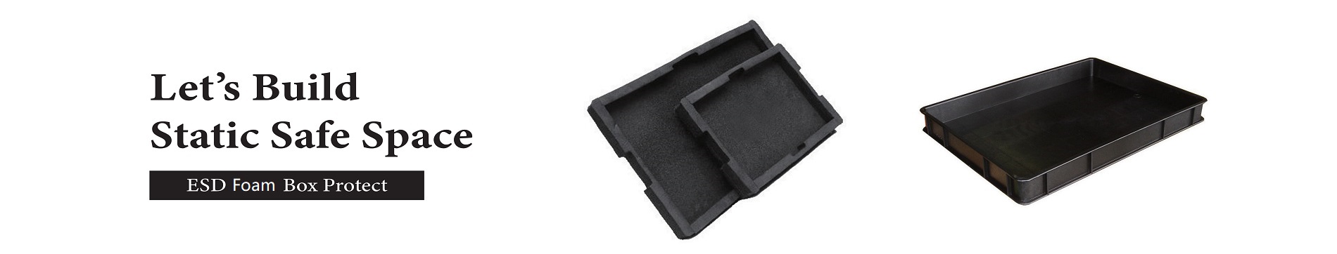
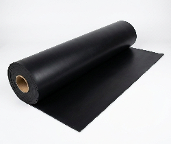
2. Introducing the Dual-Layer ESD Silicone Mat
Yufa Polymer's Your ESD Mat Is Corroding Your Products — And You Don't Even Know It was engineered from the molecular level to address all three challenges simultaneously. Rather than modifying an existing formula, we redesigned the material architecture using a proprietary dual-layer structure: premium silicone compounded with high-efficiency carbon black, forming an integrated conductive network that maintains stable electrical properties across the full operating temperature range.
The core technology can be summarized as: "Silicone matrix + carbon black conductive network + dual-layer resistance gradient control" — a design that precisely balances safe charge dissipation with rapid grounding.
3. Six Core Performance Characteristics
3.1 Dual-Layer Electrostatic Control Architecture
Unlike single-layer ESD mats on the market, this product features a precision-engineered dual-layer resistance gradient:
• Top Layer (Dissipative): Surface resistance 10⁶ – 10⁹ Ω — This range is carefully calibrated to ensure controlled charge dissipation without sudden discharge events (sparks, arcs) while avoiding short-circuit risks from excessively low resistance.
• Bottom Layer (Conductive): Surface resistance 10⁴ – 10⁶ Ω — Provides a low-resistance path from the top layer to ground, ensuring continuous and reliable static drainage. Even if the top layer's resistance drifts after extended use, the bottom layer maintains a dependable ground path.
• Volume Resistance: ≥10⁷ Ω — Guarantees bulk conductivity uniformity, preventing localized charge accumulation.
Practical significance: The dual-layer design creates "defense in depth" — the top layer controls discharge speed to protect components, while the bottom layer ensures rapid grounding for continuous safety. Static decay time meets SJ/T 11236-2001 standard at "ultra-fast" classification.
3.2 450°C Instantaneous Temperature Resistance
This is the product's most significant differentiator. While most ESD mats max out at 150–250°C, this silicone mat withstands 450°C instantaneous exposure. In practical terms:
• Soldering iron tips can directly contact the mat surface without a separator pad — improving operator efficiency
• Hot air guns, wave soldering fixtures, and BGA rework stations cause no damage to the mat
• Continuous operation at 260–350°C without cracking, deformation, or harmful gas release
Technical principle: The silicone molecular backbone consists of Si-O bonds with bond energy of 452 kJ/mol — far exceeding the C-C bonds (347 kJ/mol) in organic polymers. Combined with carbon black's thermal stabilization effect, the material maintains structural integrity at extreme temperatures.
3.3 Halogen-Free Chemistry
This is a performance characteristic many buyers overlook, but it is critical for high-reliability manufacturing. Conventional halogen-containing ESD materials release corrosive gases (HCl, HBr) when heated. These gases react with gold-plated connectors and silver-bearing components, forming metallic compound layers that increase contact resistance, cause signal distortion, or create open circuits.
This mat contains zero chlorine and zero bromine. At all operating temperatures, it produces no corrosive outgassing. For manufacturers of automotive electronics, medical devices, aerospace-grade products, and telecommunications equipment, this is an essential safeguard.
• Gold-plated connectors remain color-stable — no chloride-induced metal compound formation
• Silver-bearing components resist tarnishing — contact resistance stays within specification
• Full compliance with halogen-free requirements for export products (RoHS, REACH)
3.4 Matte, Oil-Free Surface Engineering
Standard silicone products often suffer from "oil bleed" — low-molecular-weight silicone oil migrates to the surface, creating oily residues. In cleanrooms or precision optics environments, this contamination can compromise optical elements and solder joint quality. Our product undergoes a proprietary surface treatment process that ensures long-term oil-free, non-migrating performance with a durable matte finish.
3.5 High Elasticity & Anti-Aging Formulation
Silicone inherently offers superior elasticity, and with carbon black reinforcement, the material achieves significantly enhanced tensile and tear strength. Even under prolonged thermal cycling and mechanical loading, the mat remains flat — no cracking, no curling, no deformation. For SMT lines running 24/7 operations, this means zero unplanned downtime for mat replacement.
3.6 Service Life Exceeding 5 Years — The True TCO Winner
Standard ESD mats typically require replacement every 6–12 months in high-temperature environments. This product delivers a service life exceeding 5 years under continuous high-temperature operation. Calculated on a Total Cost of Ownership (TCO) basis: even at a higher unit price, the annual usage cost is reduced by over 60% — not to mention the hidden cost of production line stoppages during replacements.
4. Application Scenarios in Depth
4.1 SMT & Electronics Assembly Lines
On SMT lines, the rework and touch-up station is where workstation materials face the harshest test. When operators use soldering irons to manually rework 0402, 0201, or even 01005-size components, the iron tip frequently contacts the mat surface. Standard ESD mats show burning and cracking marks within months under these conditions. This mat endures direct contact for years.
4.2 Semiconductor Fabrication & Packaging
Semiconductor packaging cleanrooms demand the highest standards of both environmental cleanliness and electrostatic protection. From wafer dicing to photolithography, from packaging to final testing, every step is intolerant of even microscopic ESD damage and particulate contamination. The oil-free surface ensures no volatile organic compound release into the environment, while the dual-layer ESD structure provides continuous, stable electrostatic protection.
4.3 Precision Optics Laboratories
In the production of optical components, laser devices, and fiber optic assemblies, any oil residue or particulate can degrade optical performance. The matte, oil-free surface eliminates this risk at the source while providing complete ESD protection.
4.4 High-Heat Work Zones
Including wave soldering stations, hot air gun workstations, and BGA rework positions. The common characteristic of these stations is extreme temperature with heat sources near the mat surface — conditions that ordinary materials simply cannot withstand. The 450°C temperature rating lets operators focus on their work without worrying about mat damage.
4.5 Sensitive Component Inspection & Packaging
For ESD-sensitive microchips, MEMS sensors, RF components, and similar devices, inspection and packaging surfaces must simultaneously meet both electrostatic protection and chemical inertness requirements. The halogen-free formulation ensures zero corrosion risk — making it the ideal choice for these critical applications.
5. Technical Comparison: Our Product vs. Conventional Alternatives
Performance
Standard ESD Mat
Heat-Resistant Rubber
Yufa Silicone Mat
Temp. Resistance
150–250°C
≤300°C
450°C instant.
ESD Structure
Single-layer
Single-layer
Dual-layer gradient
Halogen Content
Some contain halogen
Contains halogen
Completely halogen-free
Corrosive Outgassing
Low
High
Zero
Surface Oil Bleed
Minimal
Noticeable
None
Service Life (Hot Env.)
6–12 months
3–6 months
≥5 years
Direct Solder Contact
No
No
Yes
6. Why Choose Yufa Polymer?
• In-House R&D: Proprietary silicone + carbon black formulation refined through thousands of iterations, ensuring batch-to-batch consistency.
• Full Customization: Custom thickness, width, and shapes available. Optional ESD grounding studs with 1MΩ resistance cables.
• Quality Assurance: Every batch ships with a complete inspection report including surface resistance, volume resistance, and static decay time.
• Free Samples: Request samples for real-condition testing. We believe our data speaks for itself.
Request Technical Specifications & Free Samples Today
Email: info@yufapolymer.com | Website: www.yufapolymer.com
Our engineering team responds within 24 hours with professional technical solutions and competitive quotations.